ADS1220 Load Cell Amplifier
A custom SPI ADC board and C++ driver for high-rate strain gauge measurement
- Context
- Northwestern HAND Lab (NSF Engineering Research Center)
- Role
- Co-designer — schematic capture, PCB layout, driver development
- Timeline
- Jan. 2025 – Present
- Collaborators
- Yuchan Choi. Advised by Anthony Shilati and Luke Batteas.
Problem
Researchers across the lab use strain gauge load cells, but the commercially available amplifier modules are effectively black boxes, and the ADC-to-microcontroller interface is tedious to set up from scratch each time. The module we were using, the NAU7802, communicates over I2C and tops out at 320 SPS — far short of what the lab needed. Target: 2 kHz sampling.
Approach
The work moved through three phases: confirm the existing hardware could produce trustworthy readings at all, calibrate it properly, then replace the bottleneck.
1. Characterize the problem with the existing hardware
Built an I2C interface between a NAU7802, a Teensy, and a load cell, plus a Python script for live plotting, to confirm readings could be captured at all.
2. Calibration
Designed and 3D printed a test rig in Onshape to hang known weights.
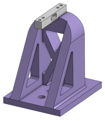
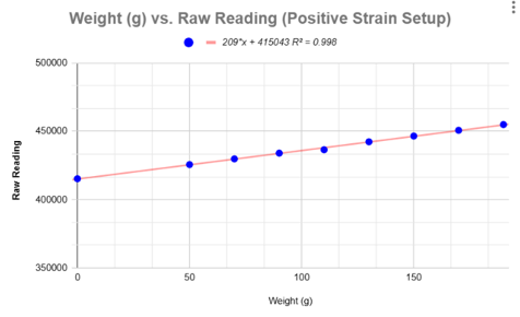
Initial readings were too noisy to be repeatable, so the calibration routine was changed to average over a 10-second window per weight, repeated 5 times per weight. Resulting fit: 209x + 415043, R² = 0.998.
3. Replace the NAU7802 with a custom board
The NAU7802’s I2C interface was the limiting factor, so the next step was a custom board built around the ADS1220, which uses SPI.
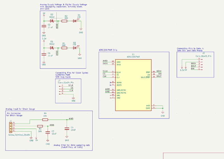
Schematic — KiCad, ADS1220 front end
PCB Design Considerations
- Anti-aliasing — passive RC low-pass filters on both analog inputs. Common-mode cutoff 994.72 Hz, sized against the 2 kHz sampling target. A differential-mode filter was added to reject inter-bridge noise. Transfer functions were modeled and Bode-plotted in MATLAB.
- Power protection — a positive clamping circuit (BZV55B3V3) on the strain gauge inputs to protect against negative voltage, plus an anti-polarity protection diode.
- Power regulation — an LP2985 low-dropout regulator to hold a stable 5V rail from a higher external supply.
- Robustness details — indicator LEDs on AVDD and DVDD, decoupling capacitors throughout, 47Ω series resistors on the SPI lines, and analog traces kept as short as possible.
- ADC clock — a 4.096 MHz PWM signal at 50% duty cycle supplied as the ADC clock.
Iteration
Two parallel board families were developed in tandem: a standalone breakout board, and a carrier board that sits directly on a Teensy.
Version A — Standalone Breakout
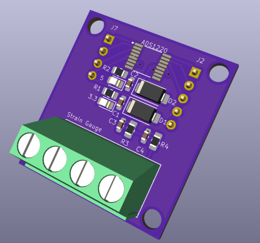
Manufactured, then found unusable on a breadboard — the M3 screw holes blocked it.
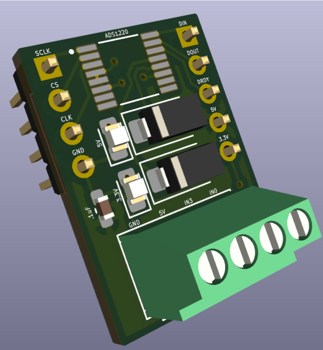
Moved components to the back of the board and dropped the screw holes to free up breadboard clearance.
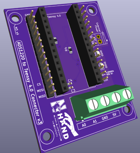
Version B — Teensy Carrier Board
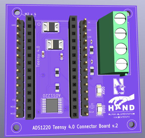
Initial mockup of the carrier-board concept.
Improved trace routing, added the external power supply path, and fixed the low-pass filter.
Video — v3 board (Version B) demoed working
Firmware
Wrote a C++ ADS1220 driver library in PlatformIO exposing begin, reset, register read/write, raw and calibrated reads, startConversion, powerDown, and findADCOffset.
findADCOffsetaverages 2000 samples to zero the load cell.resetincludes the ~1 ms delay the ADS1220 requires before it will accept any SPI command.
These boards are now used throughout the HAND Lab at Northwestern for strain-gauge data acquisition.